About three weeks ago, I helped Mike making a smart mailbox. If you haven't read his post already, it is a very nice one! Go on and read it. In short, we designed the next circuit:
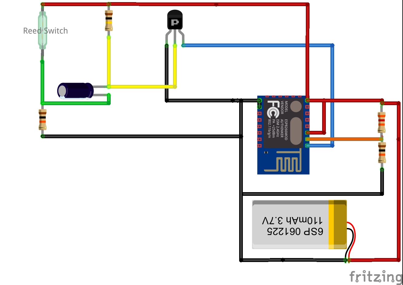 which resetting the ESP8266 every time the mailbox is opened. After the ESP8266 is reset, it sends an email using Blynk and go to deep sleep, where it draws so little current it can stay up for months using a single battery.
After finishing this project, I thought to myself that this kind of circuit can be used for many other applications such as IOT mobile alarm and more. So it seemed like a good idea to make several PCBs just like this, for other purposes. I have yet to design any PCB before, and from what I knew there were two ways to go: Homemade PCB, or designing and ordering it online.
There were pros and cons for both methods:
| Pros | Cons | |
|---|---|---|
| Homemade PCB | Fast Process (day). Mistakes can be easily fixed. |
Long time and effort for inexperience users. Bad for the environment. Usually one layer PCB only. Usually not accurate. Wires/Connectors sizes must stay relatively large. |
| Ordering Online | Easy Process (Designing only). Accurate process. Less time wasted. Less dealing with acids (is it really pro?). |
Slow process - Can take up to a month due to postal issues . Mistakes are more problematic to fix. |
This table is my point of view - Some would add more statements to some cells. Anyways, it seems pretty obvious that it is much easier and simpler to design a PCB and order it online. My problem was that I made myself a promise once that I will not order online PCB before I try to make one on my own. Since I'm usually keeping my promises I decided to go and try it out. The following post is a documentation of the process, with some errors I've done on the way, and how to fix them.
Step 1 - Designing the PCB
I started with designing the PCB using Eagle, after half an hour of watching few "Getting started" YouTube videos I was ready to start.
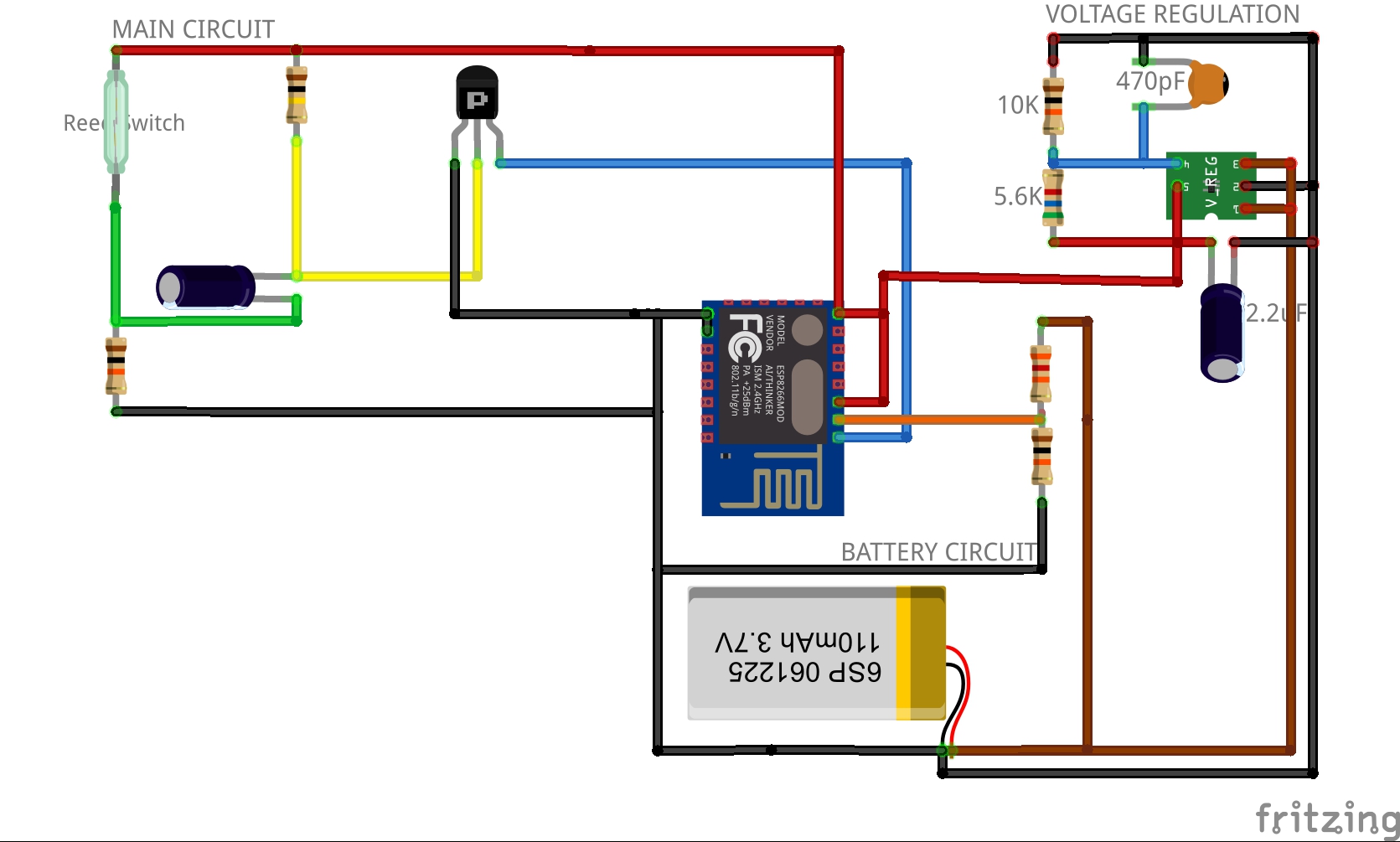
What I like about Eagle, is that you can easily design and share libraries of new components, so the first thing I've done was adding an ESP8266 library which fortunately someone has already designed, and then, I could start building my scheme. In addition to the circuit from the mailbox post I decided to add a MIC5219 voltage regulator as well. If you wonder why I use MIC5219 and not more common regulators like LM1117 check my post about measuring water temperature on the roof (In short: Dropout voltage and Power consumption).
The new circuit looked like that:
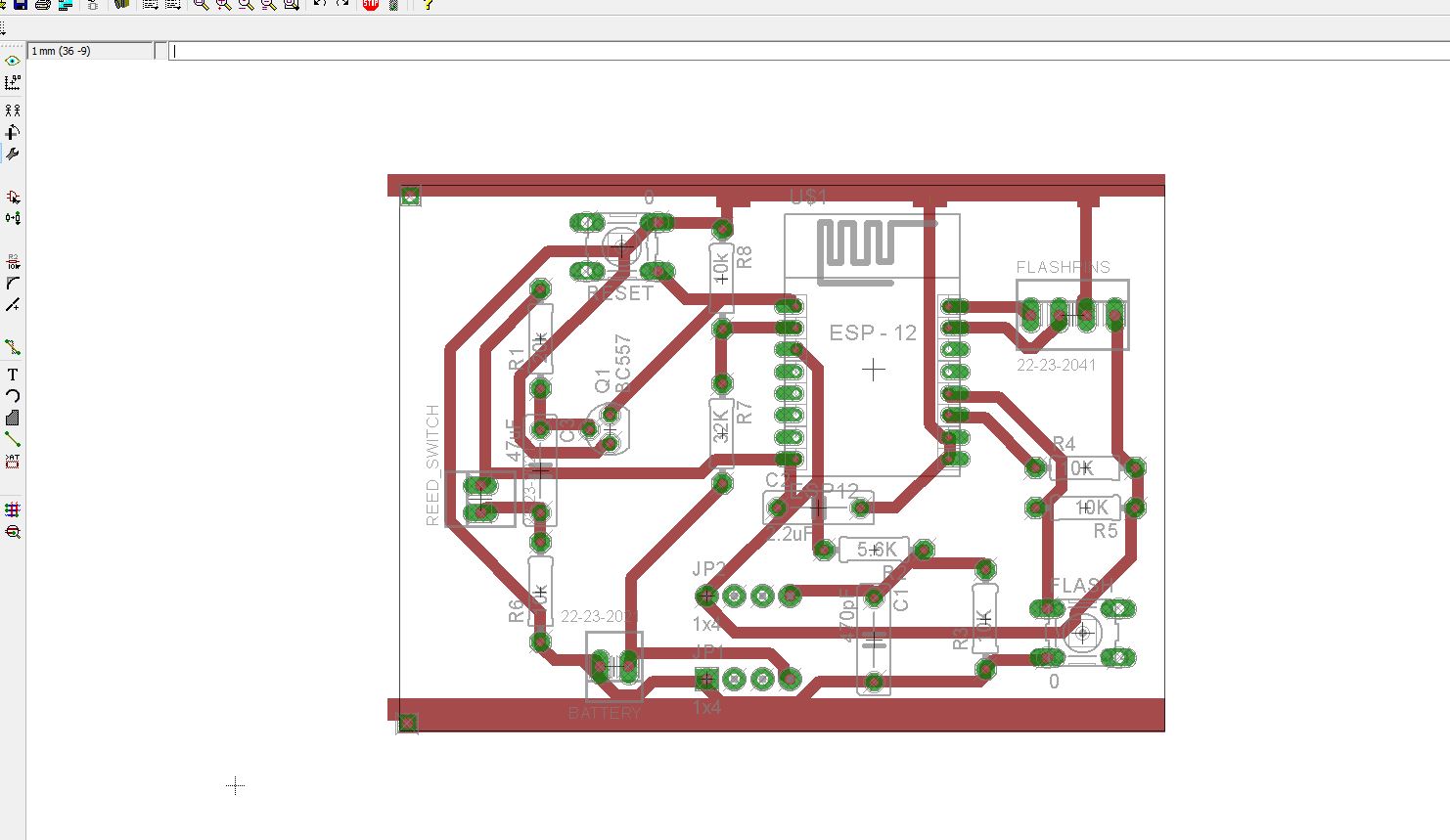
Designing a scheme is the first thing that should be done, to understand clearly all the connections on the future PCB. My final scheme looked like this:
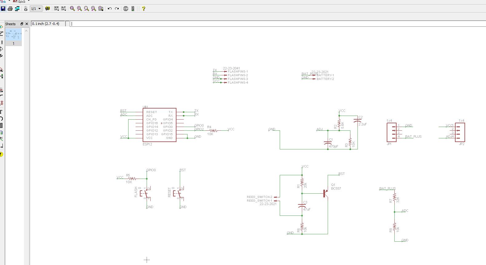
The parts of the circuit from top left to bottom right:
- Pins for flashing.
- Pins for battery connectors
- ESP8266-12 pinout, with a pull-up resistor on GPIO2.
- Circuit for the adjustment of the MIC5219 voltage regulator.
- Pins for the MIC5219 voltage regulator.
- Switch for flashing the ESP8266.
- Switch for resetting the ESP8266.
- Main circuit of the reed switch.
- Circuit for measuring the battery voltage.
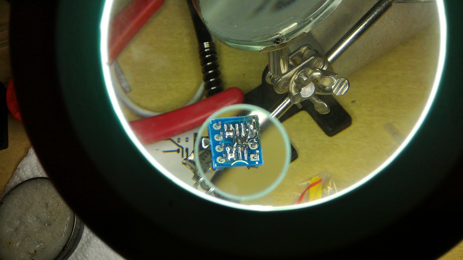
Note that I did not use the original part of the MIC5219 since it was too small for a homemade PCB. Instead, I used another board, anadapter from SOC8 to DIP8, so the MIC5219 will be soldered to this board, and this board will be soldered to the main PCB.
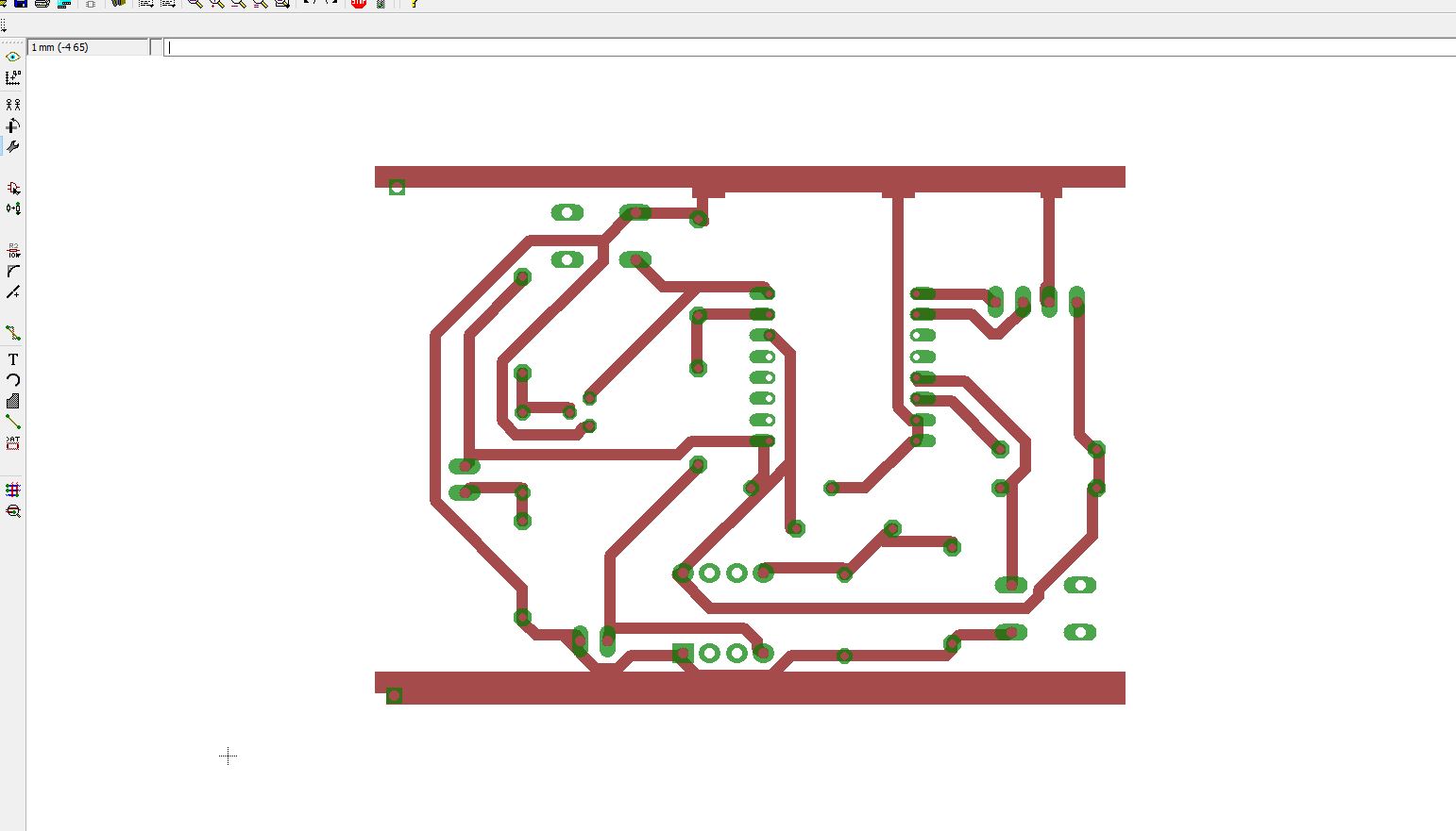
After finishing the scheme, I moved on to the board view, and placed the parts on a board of 7cm X 5cm which is the size of the copper plate I had at home. I've place the parts on the board, and played a bit with the auto-routing configurations. If you go to Edit -> Design rules, you can choose the clearance (20mil) distance (40mil) and minimum width of the wires (40mil). The numbers I chose (in bold) are just my intuition to a homemade PCB, so that the wires would be wide enough and far enough from one another. Eventually I've got to this design on the board:
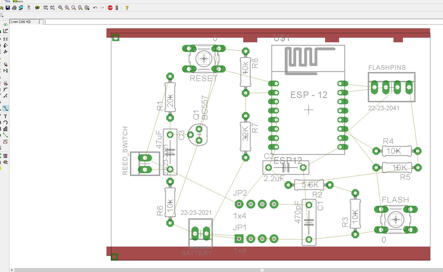
After auto-routing and some small fixes it looks like that:
An important note that should be mentioned here is that I made sure the wires wouldn't go under the ESP8266 antenna, not sure if I had to but didn't want to take a chance.
At this point I was happy with the results of the design and moved on to the next step.
Step 2 - Printing and Ironing
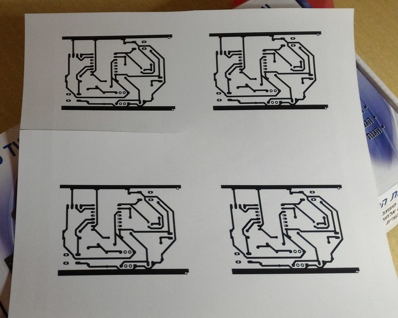
After finishing the design, I wanted to print it and pass it to the copper plate. I wanted to print several copies since I didn't know if I'll succeed on first try, so I needed to copy the sketch to a photo editor program. I started by opening the layer configuration tab on Eagle, and deselect the parts which were not supposed to be printed, so the board looked like that:
Then, I exported it as a 600dpi black and white image. It is important to keep the image in high DPI so there won't be any weird pixels on the borders of the wires.
I opened the image in Adobe Photoshop, flipped it horizontally, and duplicated it a few times.
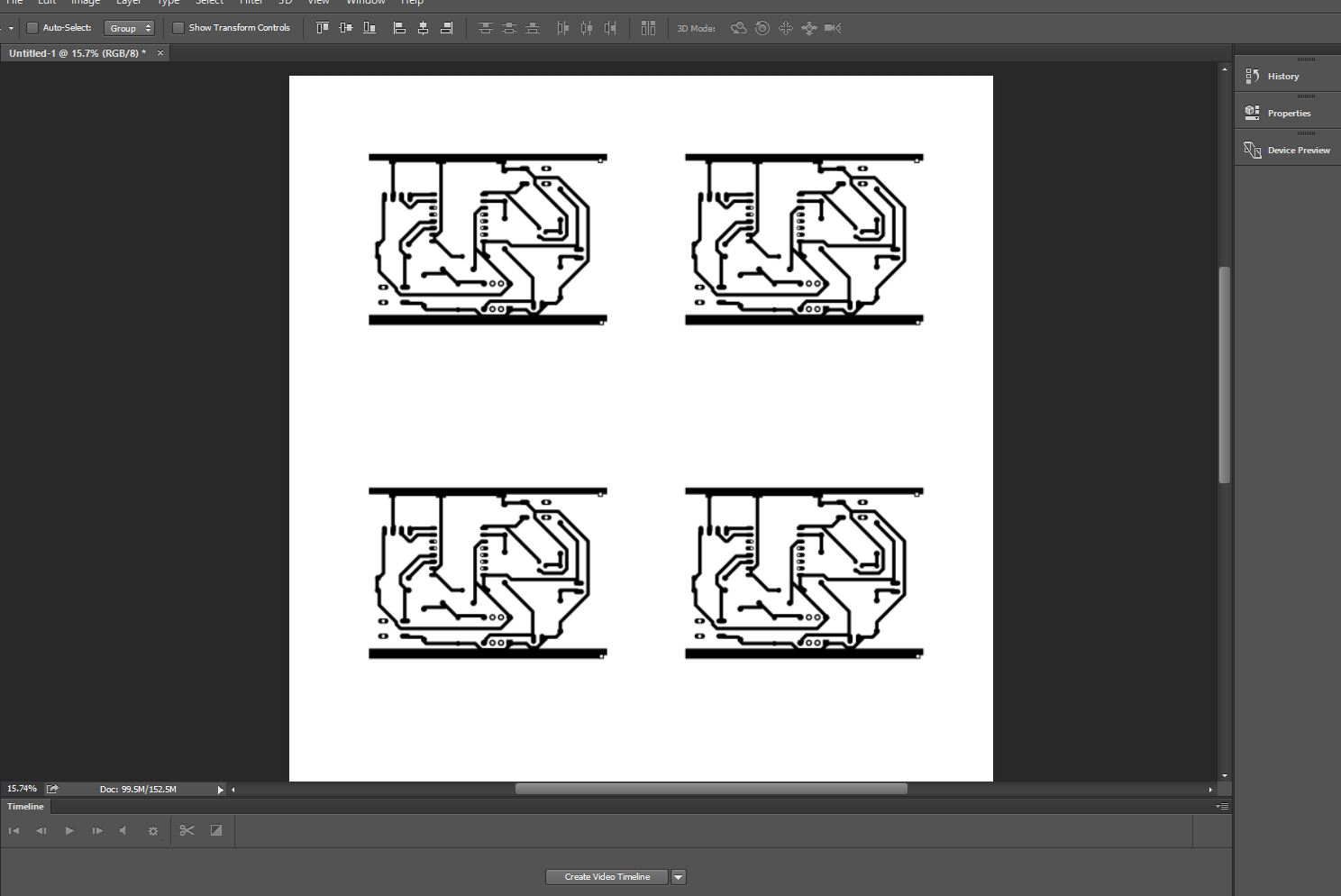
If you going to use asymmetric parts, such as the ESP8266-12, it is important to flip the image horizontally before printing. That's because after passing it to the copper image you'll also get image flipped horizontally (a mirror image) of what you've printed, so flipping it once more will result the original image.
When printing, you must use a laser printer, and it also helps using a glossy paper or any kind of paper which is not meant to be used by a laser printer. The toner of the laser printer can be removed easily from these kind of papers, and be transformed to the copper plate. The toner role is to keep the copper from dissolving by the acid later on.
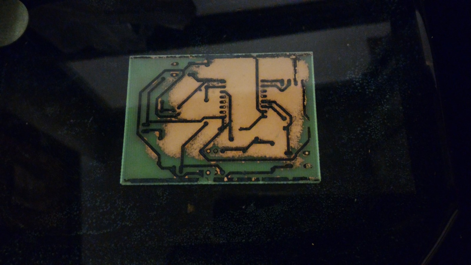
I printed the images, cut one of images, taped it to the copper plate and start ironing
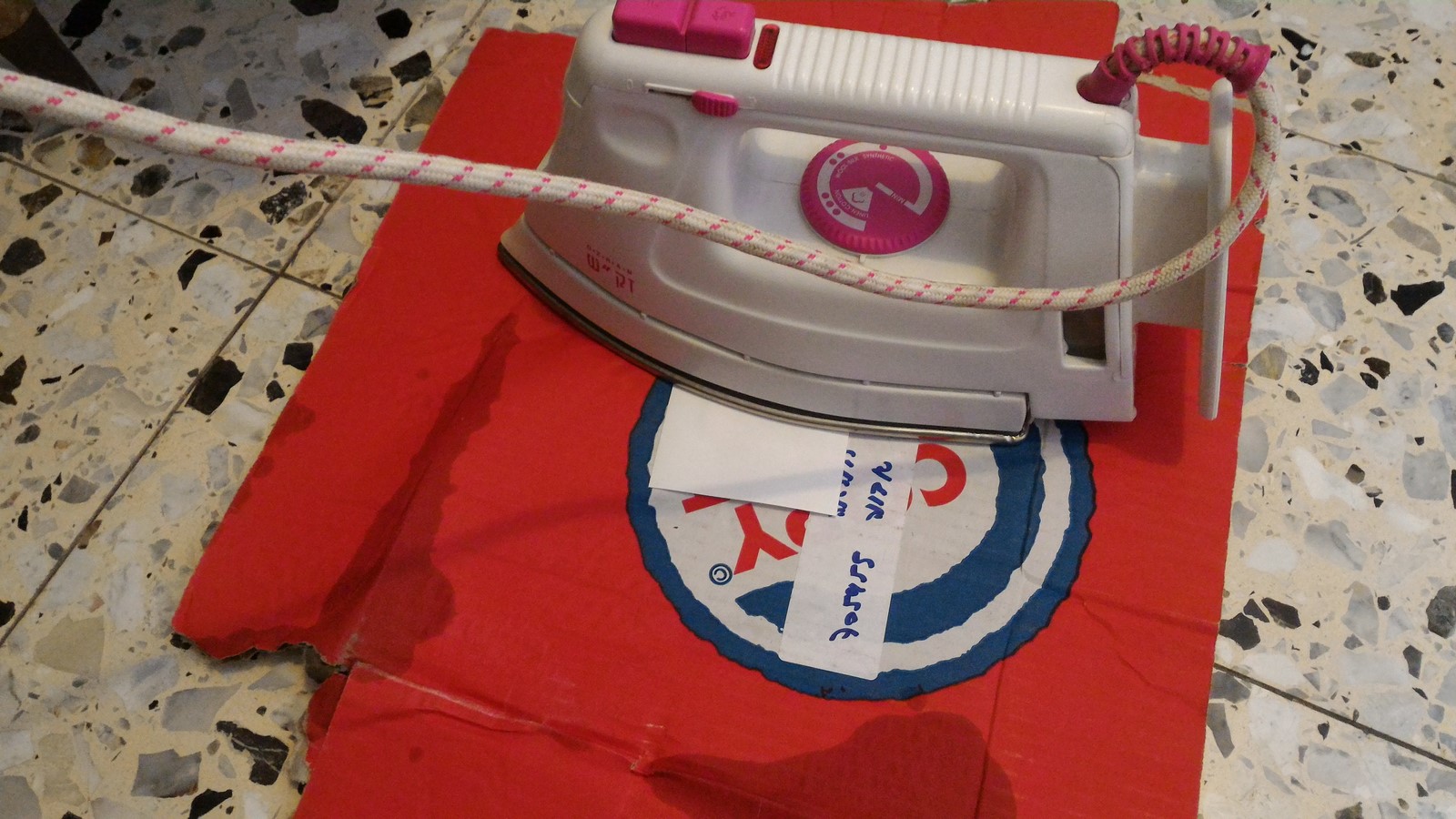
I wasn't patient enough, and apparently the iron didn't heat the entire board equally, so the first try didn't come out good, but still gave me an idea of how the this process works:
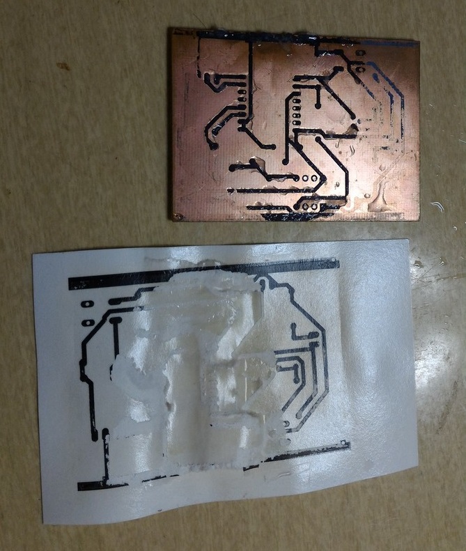
On the second attempt, I ironed the paper on the copper plate for about 10 minutes, making sure I was passing all over the paper equally. I then put it in water, so the paper will dissolve by itself
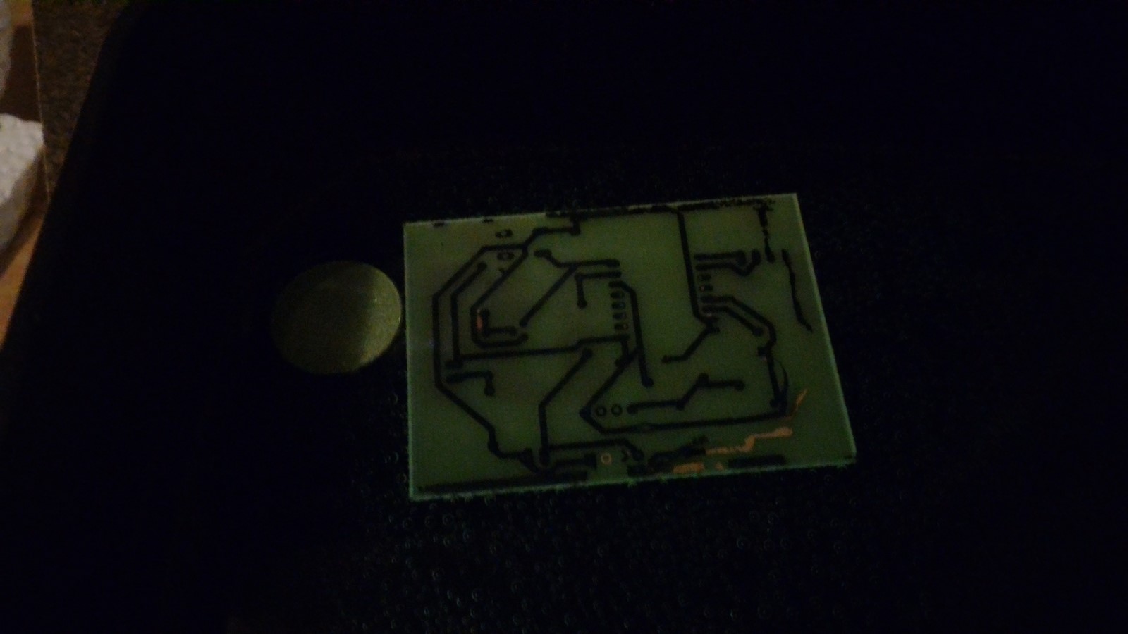
It came out very good! But then I realized that I actually forgot to make the horizontal flip on Photoshop and I got the mirror image (told you that is an important part!)
So, no rush, taking a step back, printing the images again, this time correctly
Ironing again for 10 minutes, equally all around the plate, putting in water, waiting for the paper will dissolve, and finally I got a near-perfect printing on the copper plate. At the places were the printing didn't pass well I used a permanent marker which as I read should do the same trick
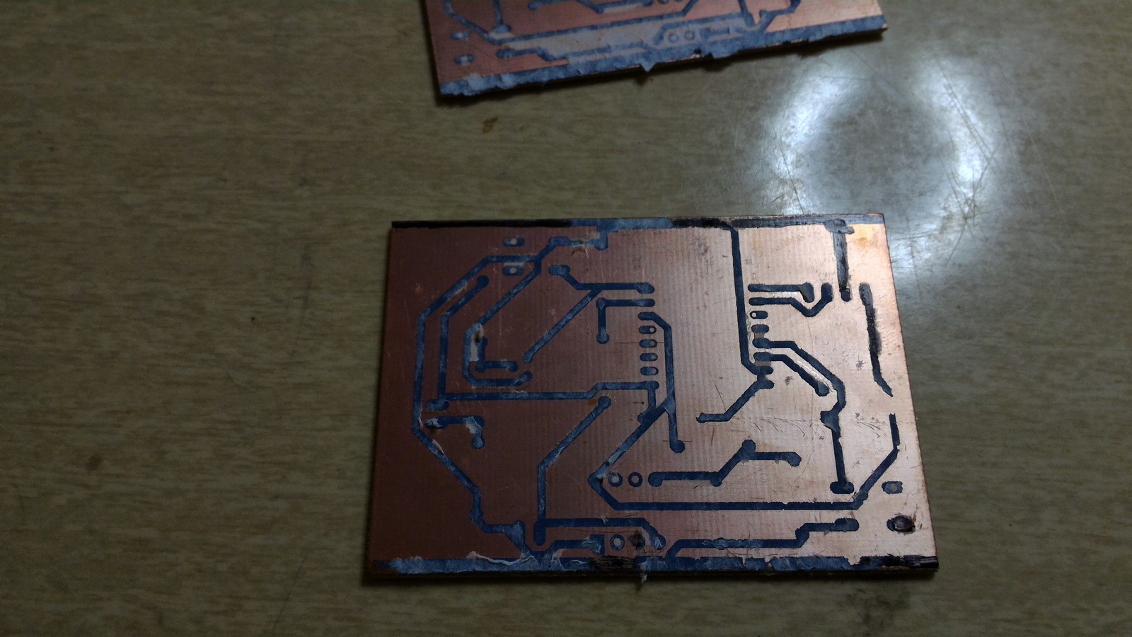
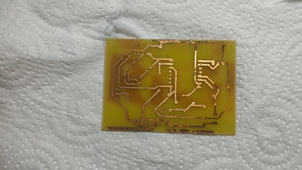
Step 3 - Removing the Copper
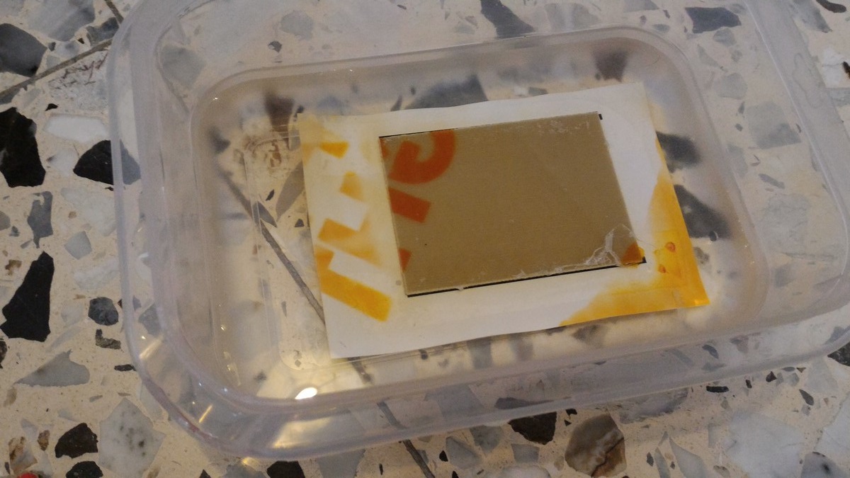
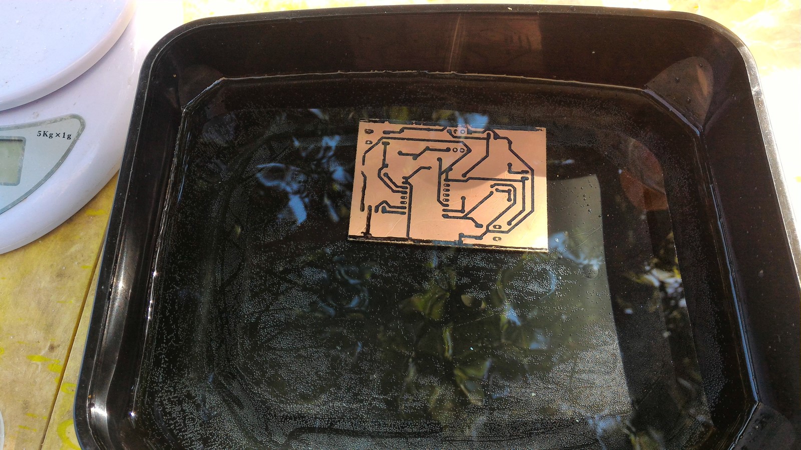
There are several acids which can be used to remove the copper. I chose this CCL blue stuff which looks like a bag of meth from the Breaking Bad TV series. The instructions were in Chinese but as far I could understand it is a bit less "bad for the environment" when disposing it. I was instructed to put a ratio of 1:10 of the acid and warm water, and wait 30 minutes. So I did
Make sure to use gloves with this acid - You don't want it on your skin.
I waited almost two hours and nothing was happening. Eventually I gave up and took out the board. It seems like some process did happened, but not something good.
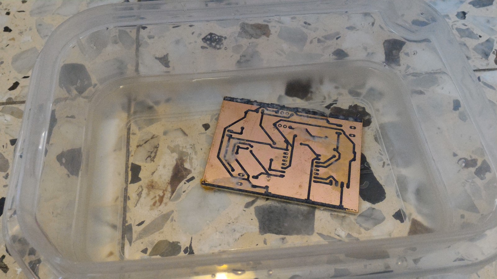
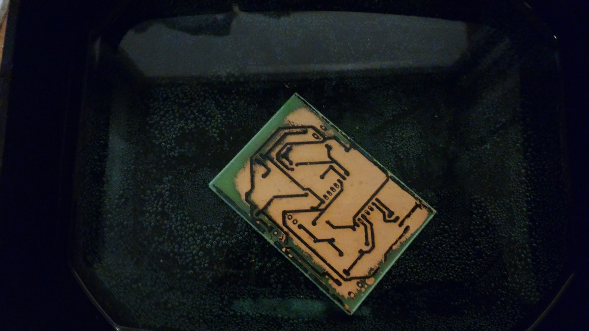
Later on, I realized I wasn't following the correct instructions. Apparently, I needed to use a ratio of 1:6 and use hot water to make the process go faster. The next day I followed the new instructions and the copper slowly slowly melted. here's some photos from the process:
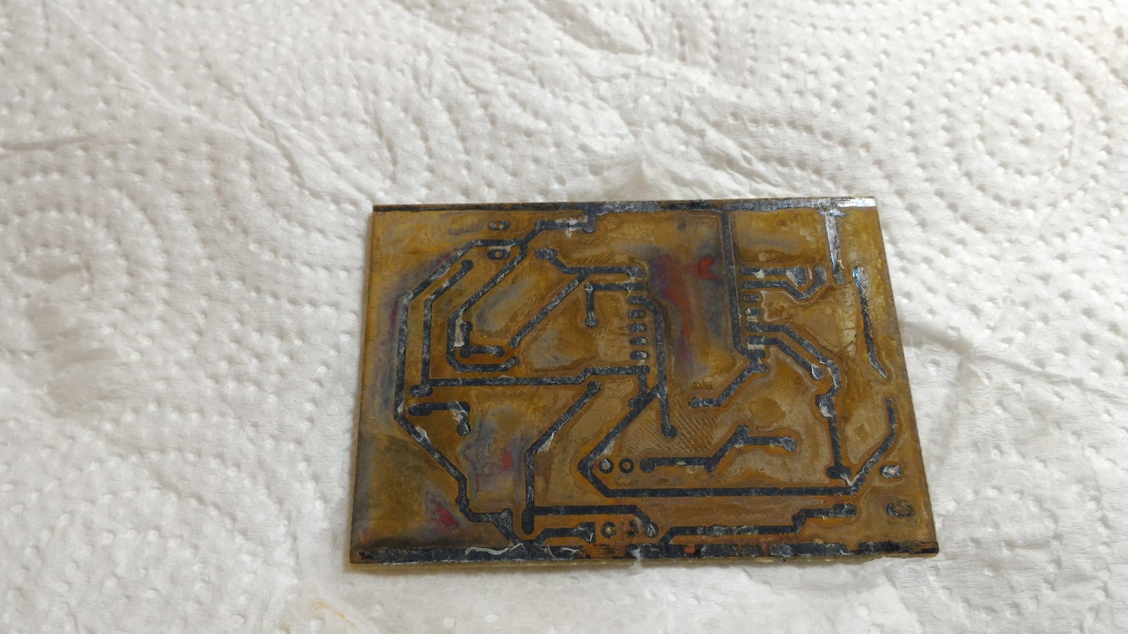
Finally, I took the board out of the acid, washed it and then removed all the toner traces using my wife's nail polish remover. If you don't have a nail polish remover any liquid with Acetone can do the trick.
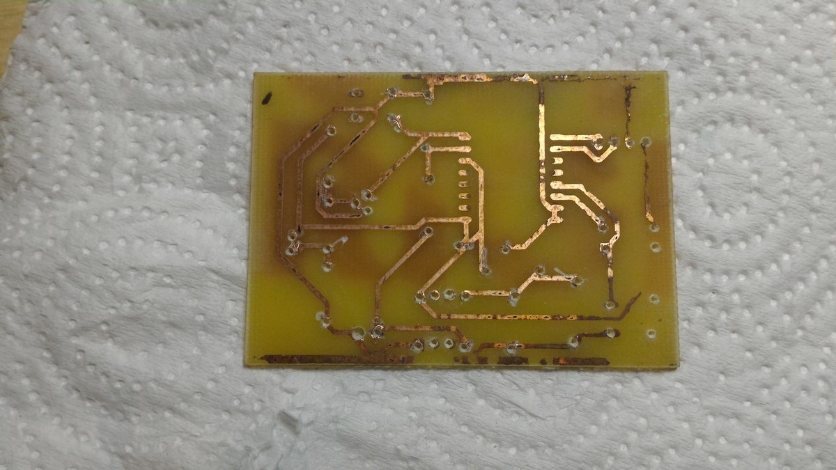
Step 4 - Drilling and Soldering
From here the steps were relatively easy. First, it is best to check that the PCB is mostly conducting. The best way doing so is to use a multi-meter, and testing that every two ends of copper stripes are conducting.
Using a Dremel and a thin bit (around 1mm) I then drilled the holes for the components. I wasn't so accurate but if the pins fit so it is accurate enough
Now it was time to solder all the components. I started by soldering the MIC5219 to its adapter, and soldering the right legs so it'll fit the PCB. It was a rather hard operation to do since it is super-tiny and my solder iron head was relatively big. Eventually, I succeeded! Turn out pretty ugly but did the work:
After that, it was time to solder all the other parts and also "fix" places where the copper was suppose to stay but was dissolved by the acid (Check the left side of the picture):
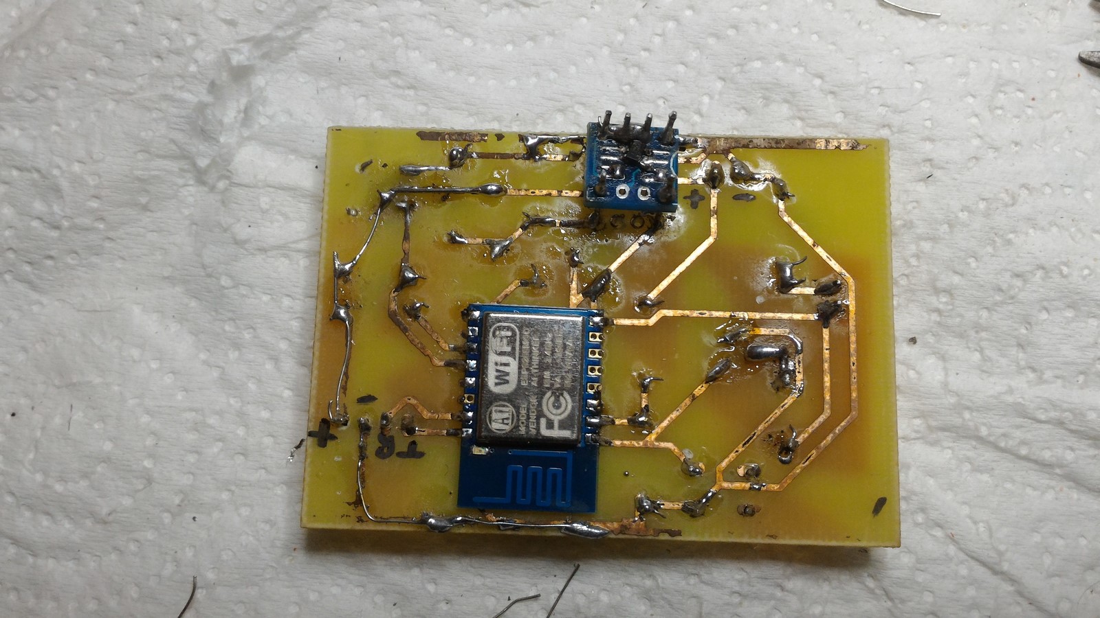
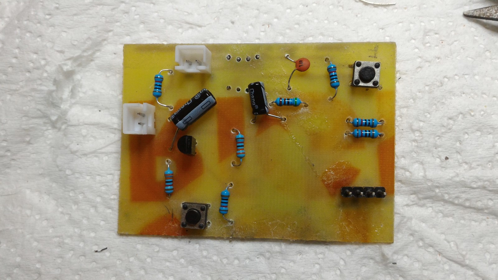
When done, I re-checked all the connections with a multi-meter and found out some wires were not conducting anymore because of the holes I have drilled. It was easily fixed by soldering some more tin around the hole and component.
Step 5 and Last - Flashing and Testing
The PCB was ready and all that left was to test it, flash it, and test it again. I started by plugging in a battery to the battery pins (I drew the plus/minus next to the pins so I won't burn the circuit by plugging it backwards). Then I tested the battery voltage, and tested there was indeed 3.3 volts at the VCC of the ESP8266. Next, I've tested the reset and flash buttons - Both were working.
So I came over to Mike's place and we began the flashing process. We plugged the FTDI to the USB and to the ESP8266 pins and flashed the program:
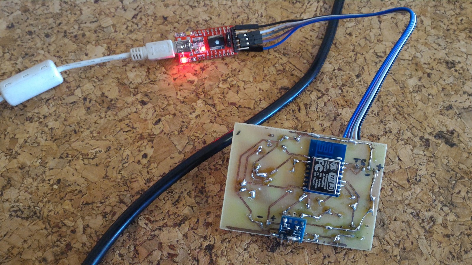
Then for the final test - We plugged in the reed switch and the battery, opened the reed switch and waited for the incoming email:
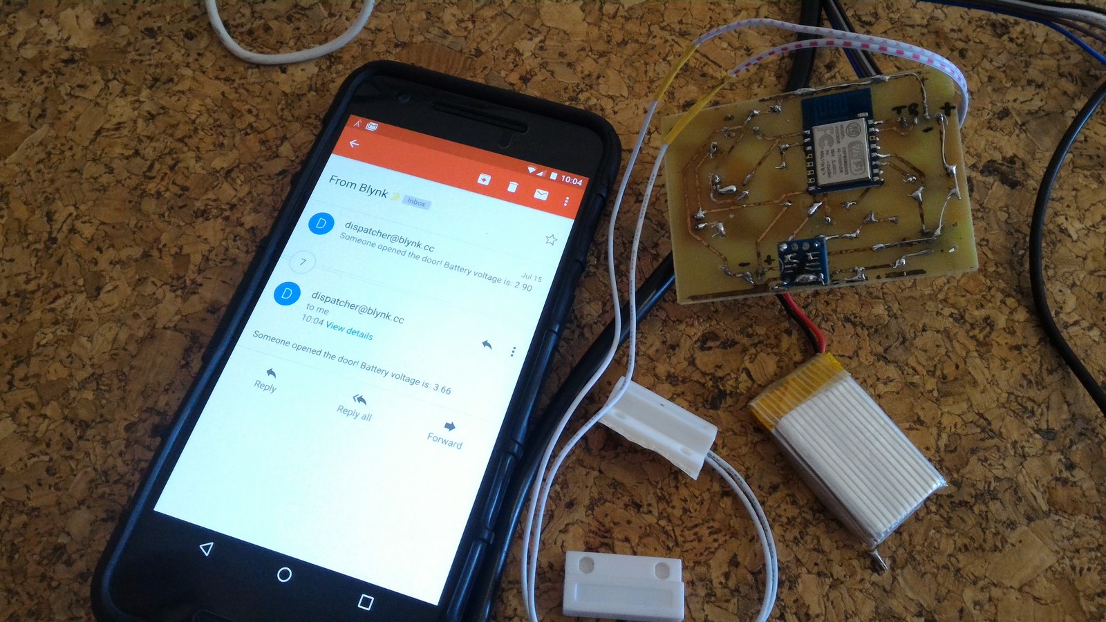
It arrived about five seconds later, showing the notification and the battery voltage - It worked!!

Looking back on this project it was a bit time consuming but educational. If I will do it again I'm pretty sure it will take less time with less mistakes. Nevertheless, the results weren't so satisfying, so next time I'm ordering my PCB from a decent factory!
All the Eagle files and the code can be found on this Github link.
AA